Read-Only Memory — universally known by its acronym ROM — is one of the most fundamental building blocks of modern computing and electronic systems. From the earliest days of digital electronics to the sophisticated embedded systems of the 21st century, ROM has played an indispensable role in storing the permanent or semi-permanent instructions that tell electronic devices how to function. Understanding ROM and its many variants is essential to understanding how computers, smartphones, gaming consoles, industrial controllers, and countless other electronic devices work at the most fundamental level.
At its most basic, ROM is a type of non-volatile memory — meaning it retains its stored data even when power is removed from the device. This characteristic distinguishes it fundamentally from RAM (Random Access Memory), which loses all stored data the moment power is cut. The non-volatile nature of ROM makes it ideal for storing firmware — the low-level software that controls hardware — and other critical instructions that a device needs to access immediately upon power-up, before any operating system or user-installed software has loaded.
The history of ROM stretches back to the earliest days of digital computing. The first ROM devices were literally hard-wired — circuits physically constructed to represent specific data values that could never be changed. As semiconductor technology advanced through the latter half of the 20th century, ROM evolved through several generations of increasingly sophisticated designs, each offering greater flexibility, higher storage density, faster access times, and lower manufacturing costs. Today, the descendants of early ROM — particularly flash memory — are among the most widely manufactured semiconductor devices in the world.
The global memory semiconductor market is enormous and growing. The total market for memory chips — including DRAM, NAND flash, NOR flash, and other ROM-derived technologies — was valued at approximately $130 billion in 2022, representing one of the largest segments of the entire semiconductor industry. Flash memory alone, which evolved directly from EEPROM technology, is manufactured in quantities of hundreds of billions of gigabytes annually to supply the insatiable demand from smartphones, laptops, solid-state drives, USB drives, and memory cards worldwide. The following sections examine each major type of ROM in detail, explaining the characteristics and operating principles of each.
Mask ROM (MROM)
Mask ROM is the original, most fundamental form of read-only memory, manufactured with its data content permanently encoded during the chip fabrication process itself. The term “mask” refers to the photolithographic masks used in semiconductor manufacturing — physical templates that define the pattern of transistors and connections etched onto the silicon wafer. In a mask ROM, the data is essentially baked into the physical structure of the chip at the foundry, with specific transistors either present or absent at each memory cell location to represent binary 1s and 0s.
Once manufactured, mask ROM data is completely and permanently fixed — there is absolutely no mechanism for erasing or reprogramming the chip under any circumstances. This absolute immutability is both its greatest strength and its most significant limitation. The strength is that mask ROM is essentially immune to accidental or malicious modification, and the stored data will remain intact indefinitely as long as the physical chip survives. The limitation is that any error in the stored data — or any need to update the firmware after manufacture — requires producing an entirely new chip at significant cost.
Mask ROM is manufactured using the same standard CMOS fabrication processes used for other integrated circuits, making it very cost-effective to produce in very large volumes once the design is finalized. Each memory cell in a mask ROM is simply a transistor that is either physically present (representing a logical 1) or absent (representing a logical 0) at a specific location in the memory array, determined irrevocably by the manufacturing mask. This simplicity allows mask ROM cells to be extremely small and densely packed, giving mask ROM very high storage density and very fast, consistent read access times.
The primary application of mask ROM has historically been in consumer electronics manufactured in very high volumes — game cartridges, set-top boxes, washing machine controllers, and similar devices where millions of identical units would use the same firmware permanently. Nintendo’s Game Boy cartridges of the 1980s and 1990s used mask ROM extensively. However, the high cost of creating new masks (which can run to tens of thousands of dollars per design) and the inflexibility of the technology have led to its gradual displacement by more flexible flash memory solutions in most applications.
Programmable ROM (PROM)
Programmable ROM, or PROM, was developed as a solution to the most significant practical limitation of mask ROM — the inability to program the chip outside of the manufacturing facility. PROM chips are manufactured in a blank, unprogrammed state with all memory cells in the same logical state (typically all 1s), and can be programmed once by the end user or device manufacturer using a specialized piece of equipment called a PROM programmer or PROM burner.
The physical mechanism by which PROM is programmed relies on tiny fusible links — microscopic electrical fuses — or, in some designs, anti-fuses, at each memory cell location. In a fuse-based PROM, all fuses are initially intact, representing one binary state. Programming is accomplished by applying a precise, elevated voltage pulse through selected fuse locations, causing those fuses to physically burn open — a permanent, irreversible change that alters the logical state of those specific memory cells to the opposite binary value. The process is called “burning” the PROM, a term that persists in colloquial use even for entirely different technologies.
The irreversibility of the fuse-blowing mechanism means that PROM, like mask ROM, can only be programmed once. Any error made during programming — a wrong bit written to any location — permanently ruins that chip, as the blown fuses cannot be restored. PROM programmers typically incorporate verification steps that check each programmed bit against the intended data immediately after writing, but errors do still occur, resulting in wasted chips. The programming process must be performed carefully and methodically, with the correct programming voltage and timing applied precisely for each device type.
PROM offered significant practical advantages over mask ROM in low-to-medium volume applications. Rather than committing to a large, expensive mask ROM production run before the firmware design was finalized, engineers could program small quantities of PROM chips themselves for prototyping, testing, and low-volume production, programming additional chips on demand as needed. This flexibility made PROM valuable in an era when firmware was often finalized late in the product development cycle, making the lead times associated with mask ROM production problematic.
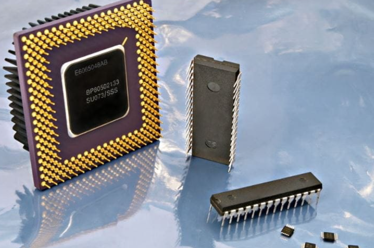
Erasable Programmable ROM (EPROM)
EPROM — Erasable Programmable Read-Only Memory — represented a major conceptual advance over both mask ROM and PROM, solving the single most frustrating limitation of those technologies: once programmed, they could never be changed. EPROM chips can be erased and reprogrammed multiple times, though the erasure process requires removing the chip from the circuit board and exposing it to a specific physical process — ultraviolet light.
EPROM chips are immediately recognizable by their distinctive quartz window — a small, transparent window set into the top of the ceramic chip package, directly above the silicon die. This window serves a specific purpose: it allows ultraviolet light to penetrate to the memory cells inside the chip for erasure. When an EPROM chip is placed in a UV eraser — a device that emits shortwave ultraviolet light, typically at a wavelength of 253.7 nanometers — and exposed for a period of typically 15 to 20 minutes, the UV photons dislodge trapped electrons from the floating gates of the memory cells, resetting all bits to the erased state (logical 1) and preparing the chip for reprogramming.
The storage mechanism in EPROM uses floating-gate MOSFET transistors — a transistor design with an electrically isolated “floating gate” between the control gate and the channel. During programming, a high voltage is applied to force electrons through a thin insulating oxide layer onto the floating gate by a process called hot-carrier injection. These trapped electrons alter the threshold voltage of the transistor, changing its logical state. Because the floating gate is completely surrounded by insulating oxide, the trapped electrons have no path to escape under normal operating conditions, giving the stored data its non-volatile character.
EPROM was invented by Intel engineer Dov Frohman in 1971, and the technology became enormously important in the electronics industry throughout the 1970s and 1980s. It made firmware development and field debugging vastly more practical than was possible with mask ROM or PROM, as engineers could erase and reprogram chips repeatedly during the development process. Intel’s 1702 was the first commercially available EPROM, storing 256 bytes — a capacity that seems laughably small by modern standards but represented valuable flexibility at the time.
The main practical limitations of EPROM were the inconvenience of the UV erasure process — requiring chip removal, UV exposure for many minutes, and reinstallation — and the gradual degradation of the floating gate oxide layer with repeated erase-program cycles, limiting most EPROMs to a few hundred to a few thousand erase cycles before reliability degraded. UV-transparent windows also added cost to the ceramic packages required. These limitations drove the development of the next generation of reprogrammable ROM.
Electrically Erasable Programmable ROM (EEPROM)
EEPROM — Electrically Erasable Programmable Read-Only Memory — solved EPROM’s primary practical limitation by enabling erasure through electrical signals rather than ultraviolet light, eliminating the need to remove chips from circuit boards for reprogramming. An EEPROM can be erased and reprogrammed while remaining in place in the target device, making it far more practical for applications where firmware updates, configuration storage, or data logging are required in the field.
Like EPROM, EEPROM uses floating-gate transistors to store data, but employs a different and more controllable charge injection mechanism — Fowler-Nordheim tunneling — to both write and erase the cells electrically. In Fowler-Nordheim tunneling, a sufficiently high electric field across a very thin tunneling oxide layer allows electrons to quantum-mechanically tunnel through the oxide barrier rather than being forced over it as in hot-carrier injection. By applying appropriate voltages, electrons can be both pushed onto the floating gate (programming) and pulled off (erasing) through the same tunneling mechanism, making the process fully electrical and fully reversible under controlled conditions.
A key characteristic of standard EEPROM is byte-level granularity — individual bytes or even individual bits within the memory array can be selectively erased and reprogrammed without affecting neighboring data. This fine-grained addressability distinguishes traditional EEPROM from flash memory (which evolved from EEPROM) and makes it well-suited for applications that require frequent, small updates to specific data locations — such as storing user configuration settings, calibration data, serial numbers, and security keys in embedded systems.
EEPROM endurance — the number of erase-program cycles the cells can survive before data retention degrades — is typically specified at 100,000 to 1,000,000 cycles for modern devices, a substantial improvement over EPROM. Data retention in a properly programmed EEPROM is typically guaranteed for 10 to 100 years, depending on the manufacturer’s specifications. These characteristics make EEPROM well-suited for applications requiring moderate-frequency updates over the life of a product.
EEPROM is extensively used today for storing small amounts of non-volatile configuration data in microcontroller-based systems — everything from the trip computer memory in automobiles to the calibration constants in medical instruments to the stored settings in industrial sensors. Dedicated serial EEPROM chips using I²C or SPI interfaces are among the most commonly used components in embedded systems design worldwide.
Flash Memory (Flash ROM)
Flash memory is the direct technological descendant of EEPROM, evolved and optimized specifically for high-density, high-speed storage in a cost-effective format. Invented by Fujio Masuoka at Toshiba in 1984 and first commercialized by Intel in 1988, flash memory has grown to become one of the most consequential semiconductor technologies ever developed, forming the foundation of SSDs, USB drives, memory cards, smartphones, and essentially all portable digital storage in the modern world.
Flash memory uses the same floating-gate transistor storage mechanism as EEPROM, with the critical architectural difference that flash cells are erased in large blocks rather than byte by byte. This block-erase architecture — which gives flash its name, from the “flash” of erasing an entire block at once — dramatically reduces the complexity of the memory array circuitry, allowing far higher storage density and lower cost per bit than traditional EEPROM. The trade-off is that updating any single byte requires erasing the entire block containing it and rewriting all the data in that block — an operation managed transparently by flash controller firmware.
There are two primary flash memory architectures — NOR flash and NAND flash — with fundamentally different internal cell organizations that produce quite different performance characteristics suited to different applications.
NOR flash connects each memory cell directly between the bit line and ground in a parallel configuration, allowing random access to any individual byte at full speed — a critical capability for code execution directly from flash (called execute-in-place or XIP). NOR flash offers fast, random read access comparable to SRAM, making it ideal for storing bootloader code and firmware that the processor needs to execute directly. However, NOR flash has relatively slow erase and write speeds and lower storage density than NAND, making it less suitable for mass data storage. NOR flash is widely used in embedded systems, automotive electronics, networking equipment, and any application requiring fast, reliable firmware storage with execute-in-place capability.
NAND flash connects cells in series strings, packing them much more densely than NOR architecture allows, at the cost of not supporting random byte-level access — data must be read in pages (typically 4KB to 16KB in size) rather than individual bytes. NAND flash offers dramatically higher storage density, lower cost per bit, and much faster sequential read and write speeds than NOR flash, making it the technology of choice for mass storage applications. Virtually all USB drives, SD cards, SSDs, and smartphone internal storage uses NAND flash. Global NAND flash production capacity is measured in exabytes per quarter — an almost incomprehensible scale of production that has driven the cost of flash storage down by over 99 percent since its introduction.
3D NAND Flash Memory
3D NAND, also called vertical NAND or V-NAND, is the most recent and most significant architectural evolution in flash memory technology, developed to overcome the fundamental physical scaling limits encountered by planar (2D) NAND flash as manufacturers attempted to shrink cell dimensions below approximately 10 nanometers. Samsung introduced the first commercial 3D NAND products in 2013, with all major flash manufacturers subsequently transitioning their production to 3D architectures.
In planar NAND flash, memory cells are arranged in a single horizontal layer on the silicon substrate. As cell dimensions shrank to improve density, the cells became so small that stored charge levels fell to just a few electrons per cell, making reliable data storage increasingly difficult and reducing endurance and retention. Rather than continuing to shrink cells horizontally, 3D NAND stacks multiple layers of memory cells vertically — current production devices stack 100 to over 200 layers, with leading manufacturers announcing designs approaching 300 layers.
By building upward rather than shrinking horizontally, 3D NAND achieves dramatically higher storage density per unit of silicon area while actually using larger cell geometries than the most aggressive planar NAND designs. The larger cells improve reliability, endurance, and data retention compared to the smallest planar cells. The combination of higher density, improved reliability, and lower cost per bit has driven essentially complete industry transition to 3D NAND architecture for new production capacity. Modern 3D NAND flash chips can store multiple terabytes of data on a single chip package, a storage density that would have been considered extraordinary just a decade ago.
Multi-Level Cell (MLC) Flash
Multi-Level Cell flash memory achieves higher storage density by storing more than one bit of data per physical memory cell, exploiting the ability to program the floating gate to multiple distinct charge levels rather than the simple two-level (charged/uncharged) approach of Single-Level Cell (SLC) flash. Standard MLC stores 2 bits per cell by programming four distinct charge levels, effectively doubling the storage density compared to SLC flash using the same cell dimensions and manufacturing process.
The penalty for this density improvement is a reduction in performance and endurance compared to SLC. With four charge levels to distinguish rather than two, the sensing circuitry must make finer measurements, increasing read latency. Programming is also more complex and slower, as cells must be carefully programmed to precise charge levels. Most significantly, endurance is substantially reduced — MLC flash typically sustains 3,000 to 10,000 program-erase cycles compared to 50,000 to 100,000 cycles for SLC flash — because the finer charge level distinctions leave less margin for the gradual oxide degradation that occurs with each cycle.
MLC flash is the standard technology in consumer SSDs, memory cards, and USB drives where cost efficiency and storage density take priority over the maximum endurance and performance offered by SLC. The consumer electronics industry has been built substantially on MLC flash economics, which has enabled the dramatic price reductions in solid-state storage that have made SSDs mainstream in laptops and desktop computers over the past decade.
Triple-Level Cell (TLC) Flash
Triple-Level Cell flash stores 3 bits per physical cell by programming eight distinct charge levels, achieving 50 percent higher storage density than MLC at the cost of further reduced performance and endurance. TLC flash typically endures 500 to 3,000 program-erase cycles — significantly less than MLC — and has slower write speeds due to the increased complexity of programming to one of eight precise charge levels. However, the substantially lower cost per gigabyte compared to MLC has driven TLC to become the dominant flash technology in consumer solid-state storage devices.
Modern consumer SSDs using TLC NAND flash compensate for the technology’s lower endurance through sophisticated controller algorithms, wear leveling, overprovisioning (dedicating a portion of the physical storage capacity as a buffer to distribute writes), and the use of high-speed SLC write caches — areas of the flash configured to operate in SLC mode temporarily to absorb burst write loads before redistributing the data more slowly to TLC cells. These techniques make modern TLC SSDs sufficiently durable for the workloads of most consumer users despite the lower inherent endurance of the underlying memory cells.
Quad-Level Cell (QLC) Flash
Quad-Level Cell flash represents the current frontier of flash density scaling, storing 4 bits per cell across 16 distinct charge levels. QLC flash achieves the highest storage density and lowest cost per gigabyte of any flash technology currently in mass production, enabling extremely affordable multi-terabyte consumer SSD capacities that were unimaginable just a few years ago. However, QLC flash has the lowest endurance of all MLC variants — typically only 100 to 1,000 program-erase cycles — and the slowest write speeds, as programming to one of 16 precise charge levels requires extremely careful, iterative charge placement.
QLC flash is increasingly common in high-capacity consumer SSDs, where the combination of large SLC write caches, intelligent controller algorithms, and the typically light write workloads of most consumer use cases (predominantly sequential reads for media consumption) make the low endurance practically acceptable. For write-intensive applications — database servers, video editing workstations, or any use case involving continuous, sustained write operations — QLC flash is generally inappropriate without very careful workload analysis, and enterprise customers typically specify MLC or SLC flash for their highest-write-intensity storage requirements.
ROM in Microcontrollers (Embedded Flash)
Modern microcontrollers — the small, integrated computing devices that control everything from automobile engine management systems to washing machines, medical devices, and industrial robots — almost universally incorporate flash memory directly on the same silicon die as the processor core, memory, and peripherals. This on-chip embedded flash serves the same function as a separate ROM chip in earlier designs, storing the program code and constant data that the microcontroller executes, but with the significant advantages of lower system cost, smaller board footprint, and faster code access compared to external memory solutions.
Embedded flash in microcontrollers is typically NOR flash architecture, enabling direct code execution from flash at speeds compatible with the processor core clock. The flash is organized into sectors or pages that can be individually erased and reprogrammed, allowing firmware updates to be applied in the field through interfaces such as JTAG, SWD, USB, UART, or over-the-air wireless connections. This in-system programming capability is essential for product lifecycle management, enabling manufacturers to issue firmware updates that fix bugs, add features, or patch security vulnerabilities after products have been deployed to customers worldwide.
ROM BIOS / UEFI Firmware
The BIOS (Basic Input/Output System) — and its modern successor, UEFI (Unified Extensible Firmware Interface) — is the firmware stored in a ROM chip on a computer’s motherboard that executes immediately when the system is powered on, before any operating system loads. The BIOS/UEFI performs the Power-On Self-Test (POST), initializes and tests the hardware components, establishes the basic input/output services available to the operating system, and locates and transfers control to the operating system bootloader.
Early PC BIOS firmware was stored in mask ROM or PROM chips that were completely fixed and could only be updated by physically replacing the ROM chip — a process requiring technical expertise and physical access to the motherboard. The adoption of flash memory for BIOS storage in the 1990s transformed firmware management, enabling BIOS updates to be applied through software utilities running under the operating system. Modern UEFI firmware is stored in SPI NOR flash chips, typically ranging from 16 to 128 megabytes in capacity, and can be updated through operating system utilities, manufacturer tools, or the UEFI interface itself.
The security of BIOS/UEFI flash has become an increasingly important concern as attackers have recognized that firmware-level malware — implanted in the BIOS flash — can survive operating system reinstallation and even hard drive replacement, providing extraordinarily persistent access to compromised systems. Modern secure boot implementations and hardware-based firmware integrity verification are designed to address these threats, though the arms race between firmware security researchers and sophisticated attackers continues to evolve.